TNO and Holst Centre facilities
Holst Centre, powered by imec and TNO, offers state-of-the-art facilities for the development of wireless sensor technologies and flexible electronics. Partners benefit from access to an extensive network of facilities, including specialised lab spaces and cleanrooms that support advanced research and development.
Learn more- Service Labs and cleanrooms
- Provider Holst Centre
- Homebase High Tech Campus 4, 11, 21, 25, 29, 31
- Phone +31 (0) 40 40 20 400
An overview of locations on Campus
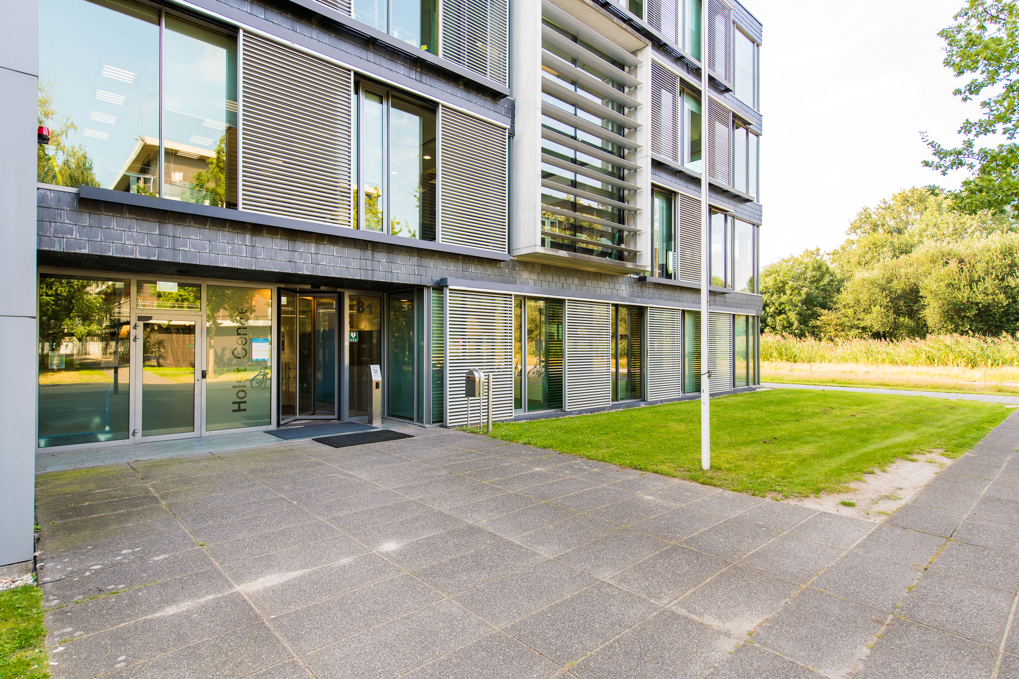
Head office – HTC 31: This is where you will find the offices and analyses labs.
Thin-film transistor labs & cleanrooms: – HTC 21: These cleanrooms and labs are optimally equipped for thin-film transistors, spatial ALD and batteries. These facilities include large-area OLED and OPD deposition tools, laser facilities, and a cleanroom plate line for maskless lithography and etching. Substrates of 15×15 cm² up to gen1 (35×32 cm²) can be used to manufacture any flexible electronic device, including displays, sensors and batteries.
TNO Material Solutions & Chemical Lab – HTC 25: Lab dedicated to the development of innovative materials with advanced functional properties. These materials offer custom-made chemical compositions and nano- or microstructures.
Hybrid Printed Electronics Lab, Chemical Labs & Cleanrooms – HTC 29: Cleanrooms and labs for Hybrid Printed Electronics. This facility features multiple roll-to-roll production lines for printing, moulding, thermoforming, laminating, coating, soldering, 3D printing and laser-transferring of flexible electronic components and systems. Flexible substrates such as foils, fabrics and paper can be used with a web-width of up to 30 cm, both R2R and S2S.